- 您现在的位置:买卖IC网 > Sheet目录341 > MAX7307AUB+T (Maxim Integrated)IC LED DRIVER LINEAR 10-UMAX
�� �
�
�SMBus/I� 2� C� Interfaced� 4-Port,� Level-Translating�
�GPIOs� and� LED� Drivers�
�WRITE� TO� OUTPUT� PORTS� REGISTERS�
�(P4)�
�SCL�
�1�
�2�
�3�
�4�
�5�
�6�
�7�
�8�
�9�
�SLAVE� ADDRESS�
�REGISTER� ADDRESS�
�SDA�
�S�
�1�
�0�
�0�
�1�
�1�
�A1�
�A0�
�0�
�A�
�0�
�0�
�0�
�0�
�0�
�1�
�0�
�0�
�A�
�MSB�
�DATA�
�LSB�
�A� A�
�P�
�START� CONDITION�
�R/W�
�ACKNOWLEDGE� FROM� SLAVE�
�ACKNOWLEDGE� FROM� SLAVE�
�STOP�
�ACKNOWLEDGE�
�P4–P1�
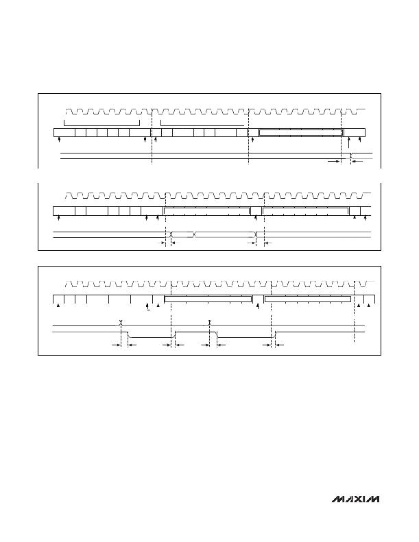
�Figure� 14.� Write� to� Output� Port� Registers�
�READ� FROM� INPUT� PORTS� REGISTERS�
�t� PPV�
�DATA� VALID�
�SCL�
�1�
�2�
�3�
�4�
�5�
�6�
�7�
�8�
�9�
�SDA�
�S�
�1�
�0�
�0�
�1�
�1�
�A1�
�A0�
�1�
�A�
�MSB�
�DATA1�
�LSB�
�A�
�MSB�
�DATA4�
�LSB�
�NA�
�P�
�START� CONDITION�
�R/W�
�ACKNOWLEDGE FROM SLAVE�
�ACKNOWLEDGE FROM MASTE� R�
�STOP�
�NO� ACKNOWLEDGE�
�P4–P1�
�DATA1�
�DATA2�
�DATA3�
�DATA4�
�Figure� 15.� Read� from� Input� Port� Registers�
�INTERRUPT� VALID/RESET�
�t� PH�
�t� PSU�
�SCL�
�1�
�2�
�3�
�4�
�5�
�6�
�7�
�8�
�9�
�SDA�
�S�
�1�
�0�
�0�
�1�
�1�
�1�
�A0�
�1�
�A�
�MSB�
�DATA2�
�LSB�
�A�
�MSB�
�DATA3�
�LSB�
�NA�
�P�
�START� CONDITION�
�R/W�
�ACKNOWLEDGE� FROM� SLAVE�
�ACKNOWLEDGE� FROM� MASTER�
�STOP�
�NO� ACKNOWLEDGE�
�P4–P1�
�DATA1�
�DATA2�
�DATA3�
�INT�
�t� IV�
�t� IR�
�t� IV�
�t� IR�
�Figure� 16.� Interrupt� and� Reset� Timing�
�same� rules� as� for� a� write.� Thus,� a� read� is� initiated� by� first�
�configuring� the� MAX7306/MAX7307’s� command� byte�
�by� performing� a� write� (Figure� 13).� The� master� can� now�
�read� n� consecutive� bytes� from� the� MAX7306/�
�MAX7307� with� the� first� data� byte� being� read� from� the�
�register� addressed� by� the� initialized� command� byte�
�(Figure� 15).� When� performing� read-after-write� verifica-�
�tion,� remember� to� reset� the� command� byte’s� address�
�because� the� stored� command� byte� address� has� been�
�autoincremented� after� the� write� (see� Table� 1).�
�Operation� with� Multiple� Masters�
�If� the� MAX7306/MAX7307� are� operated� on� a� 2-wire�
�interface� with� multiple� masters,� a� master� reading� the�
�MAX7306/MAX7307� should� use� a� repeated� start�
�between� the� write� that� sets� the� MAX7306/MAX7307’s�
�address� pointer,� and� the� read(s)� that� takes� the� data�
�from� the� location(s).� This� is� because� it� is� possible� for�
�master� 2� to� take� over� the� bus� after� master� 1� has� set� up�
�the� MAX7306/MAX7307’s� address� pointer,� but� before�
�master� 1� has� read� the� data.� If� master� 2� subsequently�
�changes� the� MAX7306/MAX7307� ’s� address� pointer,�
�then� master� 1’s� delayed� read� can� be� from� an� unexpect-�
�ed� location.�
�Bus� Timeout�
�Clear� device� configuration� register� 0x27� bit� D7� to�
�enable� the� bus� timeout� function� (see� Table� 2),� or� set� it�
�to� disable� the� bus� timeout� function.� Enabling� the� time-�
�out� feature� resets� the� MAX7306/MAX7307� serial-bus�
�interface� when� SCL� stops� either� high� or� low� during� a�
�read� or� write.� If� either� SCL� or� SDA� is� low� for� more� than�
�20�
�______________________________________________________________________________________�
�发布紧急采购,3分钟左右您将得到回复。
相关PDF资料
MAX831EVKIT-SO
EVAL KIT FOR MAX831
MAX8513EVKIT
EVAL KIT FOR MAX8513
MAX8552EUB+
IC DRIVER MOSFET HS 10-UMAX
MAX8595XETA+T
IC LED DRIVR WHITE BCKLGT 8-TDFN
MAX8607ETD+T
IC LED DRIVR PHOTO FLASH 14-TDFN
MAX8608YETD+T
IC LED DRVR WT/OLED BCKLT 14TDFN
MAX8631XETI+T
IC LED DRVR WHITE BCKLGT 28-TQFN
MAX8645YETI+T
IC LED DRVR WHITE BCKLGT 28-TQFN
相关代理商/技术参数
MAX7307EVKIT+
制造商:Maxim Integrated Products 功能描述:MAX7307 EVAL KIT/EVAL SYS - Rail/Tube
MAX730A
制造商:MAXIM 制造商全称:Maxim Integrated Products 功能描述:5V, Step-Down, Current-Mode PWM DC-DC Converters
MAX730AC/D
功能描述:直流/直流开关转换器 DICE SALES DICE RoHS:否 制造商:STMicroelectronics 最大输入电压:4.5 V 开关频率:1.5 MHz 输出电压:4.6 V 输出电流:250 mA 输出端数量:2 最大工作温度:+ 85 C 安装风格:SMD/SMT
MAX730AC/D DIE
制造商:Maxim Integrated Products 功能描述:
MAX730ACPA
功能描述:直流/直流开关转换器 5V Step-Down DC/DC Converter RoHS:否 制造商:STMicroelectronics 最大输入电压:4.5 V 开关频率:1.5 MHz 输出电压:4.6 V 输出电流:250 mA 输出端数量:2 最大工作温度:+ 85 C 安装风格:SMD/SMT
MAX730ACPA+
功能描述:直流/直流开关转换器 5V Step-Down DC/DC Converter RoHS:否 制造商:STMicroelectronics 最大输入电压:4.5 V 开关频率:1.5 MHz 输出电压:4.6 V 输出电流:250 mA 输出端数量:2 最大工作温度:+ 85 C 安装风格:SMD/SMT
MAX730ACSA
功能描述:直流/直流开关转换器 5V Step-Down DC/DC Converter RoHS:否 制造商:STMicroelectronics 最大输入电压:4.5 V 开关频率:1.5 MHz 输出电压:4.6 V 输出电流:250 mA 输出端数量:2 最大工作温度:+ 85 C 安装风格:SMD/SMT
MAX730ACSA+
功能描述:直流/直流开关转换器 5V Step-Down DC/DC Converter RoHS:否 制造商:STMicroelectronics 最大输入电压:4.5 V 开关频率:1.5 MHz 输出电压:4.6 V 输出电流:250 mA 输出端数量:2 最大工作温度:+ 85 C 安装风格:SMD/SMT